Building an HDMI capture board with the MS2109
October 15, 2026
Key points
- I designed an HDMI capture board using only ICs that JLCPCB has in stock
- The chip is the MacroSilicon MS2109 (HDMI in → USB 2.0 UVC out)
- Cross-checking against the BOM of a board I’d built before, I reused 13 of the 20 part types at the same part numbers
- The board came back, enumerated at High-Speed on the first try, and put out 1080p30 video
- I put the noise on the video down to MJPEG compression, but I’m re-checking that since publishing (see the update in the text)
Introduction
I wanted to build my own HDMI capture board.
There’s no cost argument for it at all: a commercial dongle sells for somewhere in the 1000-yen range. What I wanted was to know what’s inside one, and how much of it I could build myself.
This article records things in the order I tried them. The things that didn’t work, and the mistakes I caught partway through and fixed, are still in here — I didn’t delete them. I think it’ll be more useful to someone who wants to see the shape of the process than to someone building the exact same thing.
Every part I picked is something JLCPCB has in stock. I wanted to cut down on hand soldering, and when you’re only building one board, sourcing parts is the biggest cost there is.
👇 The PCB from a commercial dongle I took apart


What I ended up with/Schematic
The board takes video in on HDMI Type-A and streams it to the PC as a USB 2.0 UVC device. From the PC’s side it looks like an ordinary webcam.


Parts used
| Role | Part | LCSC number | Notes |
|---|---|---|---|
| Capture SoC | MS2109 | C961325 | QFN-48-EP 7×7mm |
| Firmware storage | AT24C16 | C561263 | SOP-8 I2C EEPROM |
| Step-down DC-DC ×2 | SY8089A1AAC | C479074 | Generates 3.3V and 1.2V |
| ESD array ×2 | TPD4E05U06DQAR | C138714 | 0.5pF 4ch, for TMDS |
| HDMI connector | HDMI-019S | C111617 | Type-A receptacle |
| Crystal | X322524MOB4SI | C70590 | 24MHz CL=12pF |
| Inductor ×2 | WPN4020H2R2MT | C98361 | 2.2µH / 4.3A |
| Ferrite bead ×2 | BLM18PG121SN1D | C14709 | 120Ω@100MHz |
| USB connection | 2.54mm 1×4 pin header | C5116483 | VBUS / D− / D+ / GND |
20 types and 51 placements in all; the parts came to about $5.5 per board.
The board
4-layer board, 1.6mm thick, built on JLCPCB’s standard stackup JLC04161H-7628.
| Layer | Use |
|---|---|
| L1 | Component side. All the TMDS and USB differential pairs live here |
| L2 | Solid GND. Not split |
| L3 | Power (3V3 / A3V3 / V33USB / 1V2) |
| L4 | Low-speed signals + solid GND |
Why I went with the MS2109
Listing the candidates and checking stock
I went and looked at JLCPCB’s assembly stock for real, and narrowed things down from there.
| Part number | In/out | Package | Stock | Unit price |
|---|---|---|---|---|
| MS2109 | HDMI → USB2.0 | QFN-48-EP 7×7 | 776 pcs | $2.26–3.65 |
| MS2130 | HDMI → USB3.0 | QFN-64-EP 9×9 | 663 pcs | $3.08–4.73 |
| MS2131 | HDMI → USB3.0 | LQFP-100 14×14 | 41 pcs | $4.31–6.15 |
| MS2106E | Analog → USB2.0 | LQFP-48 | No assembly stock | $1.12–1.91 |
USB 3.0 on the MS2130 was tempting, but a 9mm-square QFN-64 raises the difficulty of the board, and for a first attempt I wanted to prioritize getting something that works — so I went with the MS2109.
The MS2106E is for analog (composite / S-Video) input, which is the wrong direction for me. It wasn’t on JLCPCB’s assembly parts list either, so choosing it would have meant hand soldering.
Designs I referred to
- YuzukiHD/YuzukiHCC — an open-source MS2109 design (CERN-OHL-P). Gerbers and BOM are all there
- BertoldVdb/ms-tools — a tool for reading and writing the MS2109’s EEPROM (MIT)
I designed against the datasheet’s application circuit and these two side by side.
Key points of the circuit
Two power rails: 3.3V and 1.2V
From the 5V on USB VBUS, SY8089A1AACs make 3.3V and 1.2V.
Making the 1.2V with a linear regulator would mean (5−1.2)×0.25A ≒ 0.95W of loss and the heat that comes with it, so this one has to be a switcher.
The SY8089A1AAC’s reference is 0.6V, and the output is Vout = 0.6 × (1 + RH/RL).
| Rail | RH | RL | Calculated | MS2109 allowed range |
|---|---|---|---|---|
| 3.3V | 10kΩ | 2.2kΩ | 3.327V | 3.15–3.55V |
| 1.2V | 10kΩ | 10kΩ | 1.200V | 1.14–1.26V |
I put a 270pF Cff across RH, the upper resistor of the divider. Silergy’s application note recommends Cff=22pF for RH=100kΩ, but I scaled RH down to the 10kΩ range to match resistor values I already had, so I scaled Cff up by 10× too, to keep the zero in the same place.
Aside Why not the SY8253ADC?
I also had SY8253ADCs on hand (3A / 500kHz), but its minimum input voltage is 4.5V, which leaves no margin against the 4.40V lower limit of USB VBUS, and at 500kHz a 2.2µH inductor gives about 1A of ripple current — far too much for a 0.2A load. So I passed on it. The SY8089 takes 2.5V and up and runs at 1.5MHz, which suits bus power.
The 3.3V splits three ways through ferrites
The MS2109 has three separate kinds of 3.3V supply pins.

AVDD33 is the analog supply for the TMDS input stage, so it gets isolated from digital noise. V33USB is for the USB PHY only, and the datasheet says outright: “100nF + 10µF right next to the pin.”
AVDD12 and DVDD12, on the other hand, don’t need to be separated. The datasheet’s application circuit also ties pins 19 / 27 / 33 / 41 all to a single net called VDD12.
Decoupling goes per pin, not per rail
This is a part I recounted and fixed partway through the design.
Even on the same rail, you put one capacitor per supply pin. The point of decoupling is to kill the inductance of the current loop as seen from that pin, so a few millimetres away from the pin it stops working.
Laying out where the MS2109’s supply pins sit on the QFN, it came out like this.
| Rail | Pins | Side of the QFN | 100nF |
|---|---|---|---|
| V33USB | 6, 7, 8 | Left only | 1 (consecutive pins, effectively one node) |
| DVDD33 | 16, 23, 44 | Bottom, bottom, top | 3 |
| AVDD33 | 24, 30, 47 | Bottom, right, top | 3 |
| DVDD12 | 19, 41 | Bottom, top | 2 |
| AVDD12 | 27, 33 | Right, right | 2 |

The 1.2V is a single rail, but pin 19 is on the bottom edge and pin 41 on the top, on opposite sides of the package, so two isn’t enough — you need four.
AVDD33 is scattered across three sides too, so it needs three. My first schematic had one here, and I caught it on review.
The HDMI input
| HDMI | Connection |
|---|---|
| 1, 3, 4, 6, 7, 9, 10, 12 | TMDS 4 pairs → ESD → MS2109 |
| 2, 5, 8, 11, 17 | GND |
| 13 (CEC), 14 (reserved) | NC |
| 15, 16 (DDC) | Pulled up to HDMI +5V through 47kΩ |
| 18 (+5V) | 1kΩ → HDRXDET, 100nF → GND |
| 19 (HPD) | 1kΩ ← HDRXHPD |
Note Don’t pull the DDC lines up to 3.3V
In the HDMI spec, the sink side pulls up against the +5V the source supplies (pin 18). The MS2109’s DDC pins are 3.3V, so instead of the 1.5–2kΩ the spec assumes, you use the weak 47kΩ pull-up the datasheet specifies.
The +5V detect isn’t divided down. The 5V on connector pin 18 goes straight into HDRXDET through a 1kΩ. The design relies on the MS2109’s internal clamp plus the 1kΩ to limit the current, exactly as in the datasheet’s application circuit.
The crystal has four pads
X322524MOB4SI is an SMD3225-4P. I’d drawn it assuming two terminals, then noticed partway through and fixed it.
| Pad | Function | Connection |
|---|---|---|
| 1 | Crystal terminal | XTIN (pin 1) |
| 2 | Case (metal lid) | GND |
| 3 | Crystal terminal | XTOUT (pin 2) |
| 4 | Case (metal lid) | GND |
2 and 4 are shield terminals internally connected to the metal lid. Leave them floating and the lid acts as an antenna, which hurts the stability of the oscillator.
For the 12pF×2 load capacitors, the datasheet’s application circuit marked them NC, so I was going to DNP them at first, but I ended up fitting them. With 12pF of load capacitance on a CL=12pF crystal the frequency comes out a few tens of ppm high, but that’s not a problem for USB video.
USB goes to a 4-pin header
I dropped the Type-C receptacle and used a 2.54mm 1×4 pin header instead. The pin order is 1=VBUS / 2=D− / 3=D+ / 4=GND.
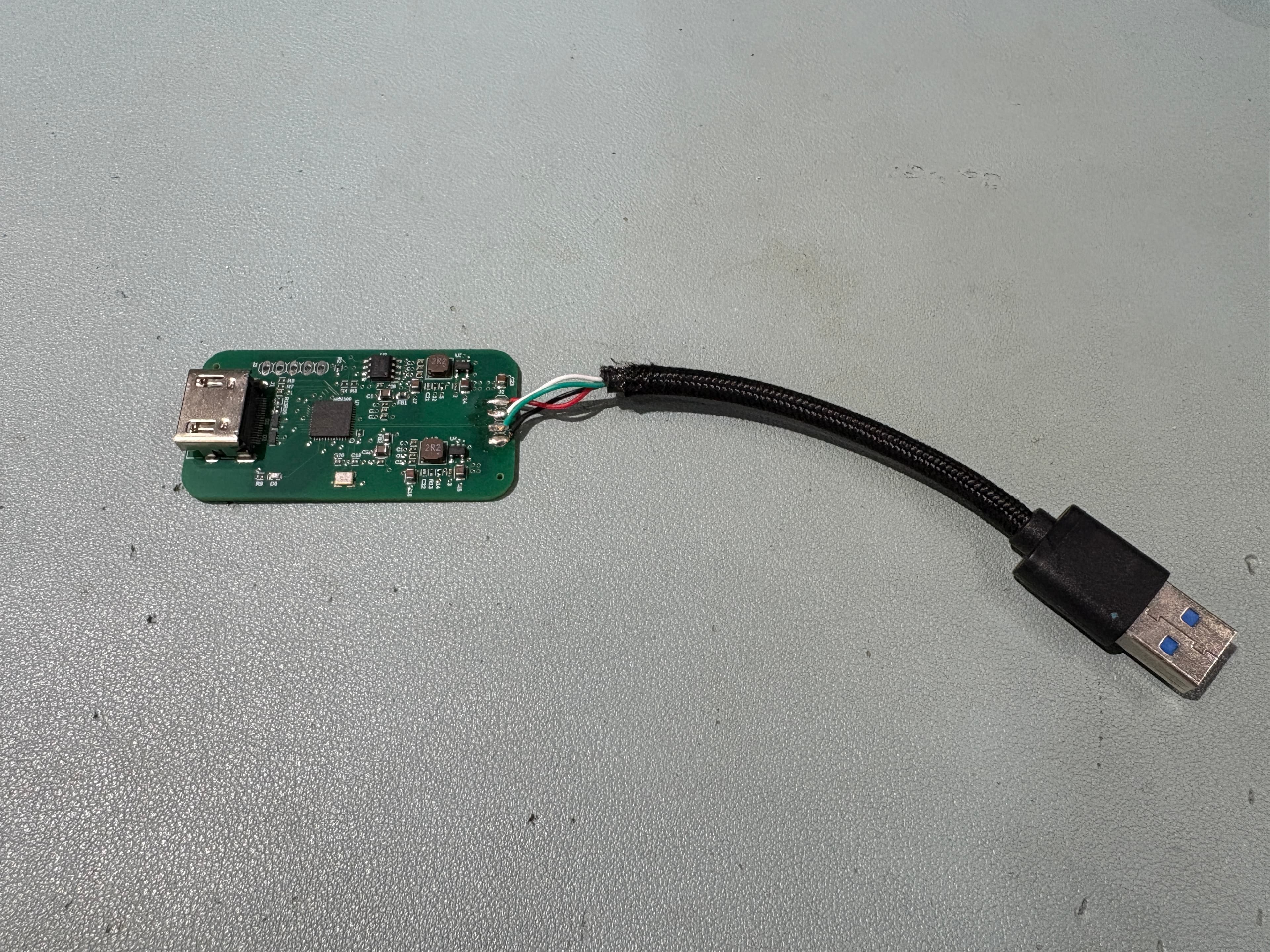
That matches the wire colour order of a USB-A cable (red, white, green, black) exactly, so if you cut up a commercial USB cable and solder it straight on, it maps 1:1.
Dropping Type-C also got rid of the two CC1/CC2 pull-down resistors.
Note USB 2.0 High Speed is 480Mbps
D± want a 90Ω differential impedance and a shield, and a pin header with jumper wires has neither. Keep the wiring under 10cm, twist D+ and D− together, and run a GND alongside. Get it wrong and High Speed enumeration fails, the device drops to USB 1.1 mode, and all you can get is 640×480.
Reusing parts from a board I built before
I had the BOM of another board I’d built previously (one with PoE and DDR4 on it) on hand, so I cross-checked against it. The result: 13 of the 20 types could be reused at the same LCSC part number.
| Reused from | → new board | What it is |
|---|---|---|
| U17, U18 | ESD array | TPD4E05U06DQAR |
| L1, L2 | Inductor | 2.2µH / 4.3A / 48mΩ |
| C11 etc. | 100nF ×15 | Murata GRM155 |
| C66 etc. | 10µF 0805 ×4 | |
| C3 etc. | 22µF 0805 ×3 | |
| C70 | 270pF ×2 | Cff for the SY8089 |
| C38 etc. | 12pF ×2 | Crystal load capacitors |
| D5 | LED | Changed to red |
| R3, R5, R9, R11 etc. | Resistors, 4 values | FOJAN FRC0402F series |
The best hit was the ESD array. I’d used the TPD4E05U06DQAR on the previous board, and it worked for TMDS as-is. It’s a part TI explicitly calls out for HDMI 2.0 in the datasheet.
I changed the design in two places to suit the reuse.
- CC resistors from 5.1kΩ to 4.7kΩ — Rd in the USB-C spec is 5.1kΩ ±20%, so that’s in range (and since I dropped Type-C in the end, it turned out not to be needed)
- FB divider from 100k/22k to 10k/2.2k — both values I already had
The parts cost went from $4.73 to $5.56, up $0.83. The Murata capacitors and the 4×4mm inductor are pricier than generic parts. It comes down to whether you’d rather standardize on fewer part numbers or keep the cost down.
The crystal I couldn’t reuse, because the previous board had an X322525MOB4SI (25MHz) and the frequency is different — but the X322524MOB4SI I picked is the 24MHz version of the same series from the same maker, YXC. The footprint and library carried over unchanged.
Board design rules
JLCPCB’s manufacturing limits and the practical line below which you don’t pay extra are two different things.
Manufacturing limits
| Item | 2-layer | 4-layer |
|---|---|---|
| Trace width / clearance (1oz) | 0.1 / 0.1 mm | 0.09 / 0.09 mm |
| Via (hole / pad) | 0.15 / 0.25 mm | Same |
Where the extra charges start
- Trace width/clearance of 3.0–3.5 mil → +20% of the order total on 4- to 8-layer boards
- Via holes under 0.3 mm → more expensive than standard
So if you stay within 5mil / 5mil and 0.3mm vias, there’s no extra charge.
What actually binds is impedance
On the 4-layer standard stackup JLC04161H-7628, the prepreg between L1 and L2 is 0.2104mm (Dk=4.4). Routing on L1 over that, the trace widths you need come out like this.
| Use | Target | Width W | Spacing S |
|---|---|---|---|
| TMDS differential | 100Ω | about 0.22 mm | about 0.18 mm |
| USB D± differential | 90Ω | about 0.24 mm | about 0.13 mm |
| Single-ended | 50Ω | about 0.35 mm | — |
Those are far wider than the 0.09mm minimum, so minimum trace width isn’t the bottleneck. The design problem isn’t being able to route thin — it’s finding the space to route at the width the impedance requires.
You can’t do this on 2 layers
For reference, here’s what the trace widths look like if you try the same thing on 2 layers.
| Construction | Dielectric thickness L1–L2 | Width needed for 100Ω differential |
|---|---|---|
| 2-layer 1.6mm | about 1.53 mm | about 2.0 mm |
| 2-layer 0.6mm | about 0.53 mm | about 0.7 mm |
| 4-layer 1.6mm | 0.21 mm | about 0.22 mm |
The MS2109 is a QFN-48 on a 0.5mm pitch with 0.25mm pads. On 2 layers you’d be connecting a trace eight times the width of the pad to a 0.25mm pad, which you simply can’t draw.

On top of that, the datasheet asks for “no routing on the layer directly under the differential traces, solid GND instead” — so if you make the whole back side of the signal layer GND on a 2-layer board, there’s no layer left to run four power rails on.
Vias
| Use | Hole / outer diameter |
|---|---|
| Standard | 0.3 / 0.6 mm |
| Crowded areas | 0.3 / 0.45 mm |
For the thermal vias in the MS2109’s EP I used 0.3mm holes / 0.6mm pads, 3×3 on a 1.2mm pitch. The EP is 5.3mm square, so they fit with room to spare.
I put no vias in the TMDS or USB differential traces. The datasheet says “two vias or fewer,” but zero is ideal.
Bringing up the board when it arrived
The board as it arrived from JLCPCB


What I did before applying power
A multimeter was the only test gear I had, so I made the pre-power checks thorough.
First I checked the part count and orientations by eye. Pin 1 markings on the QFNs, IC orientation, anything that didn’t get placed — a pass over all of it.
Next, measurements on the multimeter’s resistance range, with no power applied.
| Measurement point | Expected | Reasoning |
|---|---|---|
| VBUS ↔ GND | Several hundred kΩ or more | No DC path |
| 3V3 ↔ GND | About 12kΩ | FB divider, 10k + 2.2k |
| 1V2 ↔ GND | About 20kΩ | FB divider, 10k + 10k |
On the continuity range, I checked that 3V3↔A3V3 and 3V3↔V33USB do beep (the ferrites’ DCR) and that 3V3↔1V2 doesn’t.
I’d brought test points out on every rail, which made this part easy.
First power-up on a USB charger
HDMI stays unplugged. This board is powered from USB VBUS alone, and the +5V on the HDMI side is only used as a detect input and as the source for the DDC pull-ups, so plugging in HDMI by itself does nothing.
Worse, plugging HDMI in first means the source’s +5V goes into HDRXDET through a 1kΩ while the MS2109’s supplies are still at 0V. Putting voltage on an unpowered IC is how you get latch-up.
Before plugging it into the PC, I powered it from a USB charger. Checking the power rails only needs VBUS, so a charger with no data lines connected is plenty. If something were shorted, the only thing that breaks is the charger.
The voltages came out like this.
| Measurement point | Design value | Acceptable range |
|---|---|---|
| 3V3 | 3.327 V | 3.20–3.45 V |
| A3V3 | 3.32 V | Within 10mV below 3V3 |
| V33USB | 3.32 V | Within 10mV below 3V3 |
| 1V2 | 1.200 V | 1.16–1.24 V |
All five points were in range.
Plugging it into the PC
I’d fitted the EEPROM blank, so the question was whether it would come up on the default settings in the MS2109’s internal ROM.
Here’s what USB Device Tree Viewer showed.
Output USB Device Tree Viewer
Vendor ID : 0x534D (Hefei Macrosilicon Technology Co., Ltd.)Product ID : 0x2109Manufacturer String : "MACROSILICON"Product String : ---USB Version : 2.0 (480 Mbit/s)Device Connection Speed : High-SpeedVideo : UVC Version 1.00 -------- Default Video Modes --------1920 x 1080 @ 30 fps : MJPEG1920 x 1080 @ 5 fps : YUY21600 x 1200 @ 30 fps : MJPEG1600 x 1200 @ 5 fps : YUY21280 x 1024 @ 30 fps : MJPEG1280 x 1024 @ 8 fps : YUY21280 x 960 @ 30 fps : MJPEG1280 x 960 @ 8 fps : YUY21360 x 768 @ 30 fps : MJPEG1360 x 768 @ 8 fps : YUY21280 x 720 @ 30 fps : MJPEG1280 x 720 @ 10 fps : YUY21024 x 768 @ 30 fps : MJPEG1024 x 768 @ 10 fps : YUY2800 x 600 @ 30 fps : MJPEG800 x 600 @ 20 fps : YUY2720 x 576 @ 30 fps : MJPEG720 x 576 @ 25 fps : YUY2720 x 480 @ 30 fps : MJPEG, YUY2640 x 480 @ 30 fps : MJPEG, YUY2
What I could read out of that.
- Device Connection Speed is High-Speed — the D± routing and impedance are fine
- Product String is empty — confirms the EEPROM is unwritten (as planned)
- The resolution list matches datasheet §6.4 Table 6.3 exactly — the ROM is booting properly and emitting the right UVC descriptors
With an HDMI source connected, I got 1920×1080@30 video.
Chasing down the noise in the video
Update (October 2026)
After publishing, I re-soldered the USB cable to the board and the noise appeared to clear up. The conclusion in this section — that MJPEG compression was the cause — is being re-checked.
I’m separating the two by comparing against the uncompressed YUY2 modes and by stressing the solder joints mechanically. I’ll add the result here once I have it.
I had video, but there was coloured noise on the picture.
Capturing the PC desktop, small text came out stained magenta and cyan. I wanted to separate bad TMDS routing from USB transfer errors, so I went and looked at the pixel values in the captured image.
Looking at the numbers
| Measurement | Result |
|---|---|
| RGB of black text | (22, 22, 23) |
| RGB of a magenta area | (246, 167, 247) |
| Distribution of R − B | Mean −0.2 |
The black text is perfectly neutral. If one of the TMDS channels were down, there’d be colour here.
In the magenta areas R and B are almost identical (246 and 247) and only G is about 80 lower. And the mean of R − B is −0.2 — meaning R and B track each other perfectly.
On top of that, zooming in on large text, the edges are pure black with no colour fringing at all. White backgrounds stayed pure white too.
In other words, luma (Y) is completely intact, and only the chroma (Cb/Cr) is breaking down, and only where the text is fine.
If there were a problem with the TMDS routing or impedance, you’d see sparkle or horizontal streaking on large black fills and edges as well. If it were a USB transfer error, flat white areas would break up in blocks too. Neither was happening.
It was MJPEG compression
To push 1920×1080@30 through USB 2.0, the MS2109 compresses with MJPEG.
- Uncompressed, that’s 1920×1080×2byte×30fps = 124 MB/s (about 1Gbps)
- The usable bandwidth of USB 2.0 High-Speed is about 20 MB/s
- So the compression ratio is about 6:1

On live-action footage 6:1 is essentially lossless, but on fine text it bites. Chroma subsampling sits on top of that, so colour information is the first thing sacrificed. Magenta and cyan alternating is exactly what that failure mode looks like.
And what I was displaying this time was a PC desktop: small text tiled across the whole screen, the worst possible subject for MJPEG.
The resolution list had the answer all along
Once I’d figured that out, I went back and looked at the UVC resolution list, and there was a pattern to the frame rates attached to the YUY2 (uncompressed) modes.
| Mode | Data rate |
|---|---|
| 1920×1080 @5 YUY2 | 20.7 MB/s |
| 1280×720 @10 YUY2 | 18.4 MB/s |
| 640×480 @30 YUY2 | 18.4 MB/s |
They all land at about 18–21 MB/s. That’s the ceiling of USB 2.0 High-Speed’s usable bandwidth, and MacroSilicon had picked the fps values to fit inside it.
What to do about it
Use a YUY2 mode and you get lossless capture.
| Use | Recommended mode |
|---|---|
| PC screen, reading text | 1920×1080 @5 YUY2 |
| PC screen, some motion | 1280×720 @10 YUY2 |
| Games, video | 1920×1080 @30 MJPEG |
Commercial MS2109 dongles show the same symptom, so there was nothing particularly wrong with this board.
If you want to solve it properly, the only option is the USB 3.0 MS2130.
Things I haven’t checked yet
- Writing the EEPROM — the Product String is still empty. Write it with ms-tools and the product name and EDID can be my own. The image quality won’t change, though (the compression ratio is set by the bandwidth)
- Audio — whether it shows up as a UAC device
- Four simultaneous captures — from what I’ve read, the UVC isochronous bandwidth reservation looks like the wall here. USB 2.0 can allocate 384Mbps to isochronous traffic, while a single UVC device declares a maximum of 196Mbps. One device takes half the budget, so a second one just barely fits and a third gets rejected outright. The awkward part is that the reservation is made against the declared figure, not what’s actually consumed
Summary
- Checking JLCPCB’s stock one part at a time means nothing stalls when you place the order
- Cross-checking against the BOM of a board I’d built before, 13 of the 20 types could be reused at the same part number
- A datasheet’s application circuit looks like just a schematic, but the design intent shows up in how the nets are named (VDD12 as a single net, AVDD33 and DVDD33 kept separate)
- Do the first power-up on a USB charger. There’s no reason to put a PC port at risk
- The noise in the video wasn’t a board fault, it was MJPEG compression. Measure the pixel values and you can tell the cause apart by whether it’s luma or chroma that’s broken
I think the reason my first 4-layer board worked on the first try is that I followed §11 of the datasheet, “PCB Design Notes,” without arguing with it. Differential impedance, the number of vias, and not splitting the solid GND. Keep those three and even an amateur can get signals through at HDMI speeds.
Reference links
- MacroSilicon MS2109 datasheet
- YuzukiHD/YuzukiHCC — open-source MS2109 design
- BertoldVdb/ms-tools — analysis of the MS2106/MS2109/MS2130 and EEPROM writing
- TPD4E05U06 datasheet (TI)
- Controlled Impedance PCB Layer Stackup (JLCPCB)
- PCB Capabilities (JLCPCB)
- Multiple UVC cameras on Linux: an unexpected challenge
- USB Device Tree Viewer